2D Materials: Key Insights into Atom-Thin Chemistry
Introduction
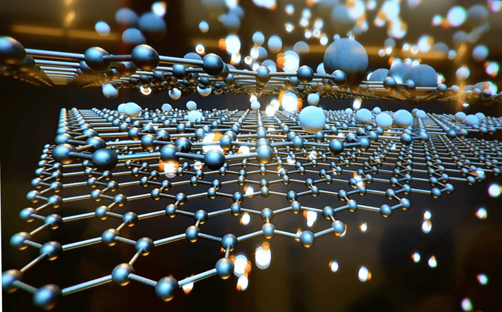
In two-dimensional (2D) materials, the structure is very thin, usually made up of just one layer of atoms. Researchers are changing how they look at electronics, photonics, energy storage, and other areas of advanced technology because these materials have properties that are very different from their bulk cousins. Many other 2D materials, such as transition metal dichalcogenides (TMDs), MXenes, and hexagonal boron nitride (h-BN), have been studied because of graphene, which is the most well-known example. Each new material has its own special properties, such as being very good at conducting electricity or very strong mechanically, and can be used in a lot of different ways.
Even though these materials show a lot of potential, scientists still have a long way to go before they can be mass-produced, the quality of the layers they make can be controlled, and these fragile structures can be used with current manufacturing methods. Stability in the real world and successful doping strategies are also problems that never go away. Still, more study has led to many important discoveries, such as layer stacking and moiré patterning, which open up new uses for 2D materials in areas as different as developing flexible electronics and quantum devices.
History
Since 2004, when graphene was first isolated, 2D materials have come a long way. Scientists were quickly interested in this single layer of carbon atoms arranged in a hexagonal lattice because it was very strong, flexible, and good at conducting electricity. The finding of graphene showed that stable, truly two-dimensional crystals could be separated, which was thought to be hard to do before. This new information led to a huge search for other 2D shapes.
Soon after, there was a lot of research, which led to the discovery of many more single-layer materials. One of the most important discoveries was that each 2D material could have qualities that couldn’t be seen in its bulk form. Some transition metal dichalcogenides, for example, have a straight bandgap when they are in their single-layer form, which makes them useful for new optical and electronic uses. Within a few years, more than a thousand projected and synthesized 2D materials were known. The field has continued to grow quickly since then.
Types of Two-Dimensional Materials
Graphene

Graphene is still the most famous 2D material. It is a sheet of carbon atoms grouped in a honeycomb pattern. It is famous for being very strong, good at conducting heat, and easy for electrons to move around in. Graphene doesn’t have a natural bandgap, but it is almost clear and very flexible, which makes it useful in flexible electronics, sensors, and high-frequency electronics. To give graphene new functions, researchers have also thought about adding other materials to it or doping it with them.
MXenes
MXenes are a big group of two-dimensional materials that are mostly made up of transition metal carbides and nitrides. People are interested in them because they carry electricity well and their surface chemistry can be changed. Because of these traits, they show promise for use in sensors, blocking electromagnetic interference, and especially in batteries and supercapacitors, which store energy. MXenes can quickly move ions around in their layered structure, which is a key part of their ability to charge quickly and store a lot of energy.
Other Emerging 2D Materials
TMDs like molybdenum disulfide (MoS₂) and tungsten disulfide (WS₂), which are semiconducting, are part of a growing library of 2D materials. These include graphene and MXenes. These work well with transistors, photodetectors, and bendable electronics in particular. Hexagonal boron nitride (h-BN) is often used as an insulating layer because it has a big bandgap, is chemically stable, and is a great dielectric. Researchers can now make moiré patterns by stacking these materials at slight rotational angles, thanks to new layering methods. This creates new quantum phenomena and tunable electronic behaviors.
Synthesis Methods
Top-Down Methods
In top-down synthesis, tiny layers are taken out of a parent crystal that is bigger.
Mechanical Exfoliation: This is one of the easiest ways to do it. You just have to use force to peel layers off of a bulk crystal. It was famously shown that you could separate graphene from graphite using sticky tape. Mechanical peeling makes high-quality sheets, but only a small amount at a time, which makes it less useful for mass production.
Chemical Exfoliation: Solvents or intercalating agents are used in chemical exfoliation to separate layers in large materials. Sonication, which uses sound waves to make mechanical energy, can help separate the layers in liquid-phase exfoliation. This method can be used on a larger scale than pure mechanical methods, but adding flaws and changing phases can sometimes change the properties of the finished material.
Bottom-Up Methods
Bottom-up methods build 2D things one atom or molecule at a time.
Chemical Vapor Deposition (CVD): Here, gaseous precursors combine with a hot substrate to form thin films. This method can make high-quality monolayers of materials like graphene or TMDs that cover a wide area. But it’s still hard to keep domain orientation and flaws under control, especially for devices that need uniform electrical properties.
Molecular Beam Epitaxy (MBE): In MBE, atoms or molecules are deposited on a substrate to make very thin layers. This is done in an ultrahigh vacuum setting. It gives you exact control over the composition, doping, and thickness. Even though MBE methods can make perfect films, they are usually slow and expensive, which makes them hard to use on a large scale.
Laser Directed Synthesis: A laser beam is used to split or make 2D nanosheets from different types of materials. By changing things about the laser, like its intensity and wavelength, experts can change the layers’ thickness and structure. This method can be very helpful for quickly and directly patterning big areas as well.
Challenges and Limitations
Scalability and Quality Control
Making a lot of consistent, high-quality 2D objects is one of the most important problems that needs to be solved right away. Some techniques, like mechanical or chemical exfoliation, can make great samples, but they’re hard to use on the large scale needed by industry for wafer-sized surfaces. Techniques like CVD can make areas that are bigger, but they can also add flaws and grain limits that make it hard for electrons to move. Achieving uniformity across big substrates while keeping high crystallinity and few defects is key to using 2D materials successfully in real-world devices.
Integration Challenges
Adding 2D materials to current gadget designs and silicon-based processes makes things more complicated. Every 2D material-based part has to connect to its surroundings, which is usually made up of regular 3D materials. Engineers need to make sure that junctions are smooth, have low contact resistance, and join well. As production moves from college labs to foundries, manufacturing lines need to be updated to handle materials that are very reactive or sensitive to air and moisture.
Stability and Longevity
A lot of 2D materials can break down in the world. Oxygen, air, or even light can change their electrical properties or make them flawed. To keep their purity, protective coatings, inert environments, and encapsulation have all been looked into. However, each has pros and cons in terms of performance, cost, and complexity. Strong long-term stability is especially important for uses where devices need to work in normal settings for a long time.
Application-Specific Limitations
Each 2D material is made for a different purpose, and it takes more than one method to make these very thin crystals work for certain jobs. For example, to doping a 2D semiconductor effectively may require complicated steps that can accidentally introduce flaws or lower the quality of the material. For optical uses, materials need to have the right bandgaps, high modulation depths, or strong nonlinear reactions. To do any of these, the chemicals and structures need to be carefully changed. To make 2D materials better for real-world technologies, we need to do more study on doping strategies, defect engineering, and interface design.


